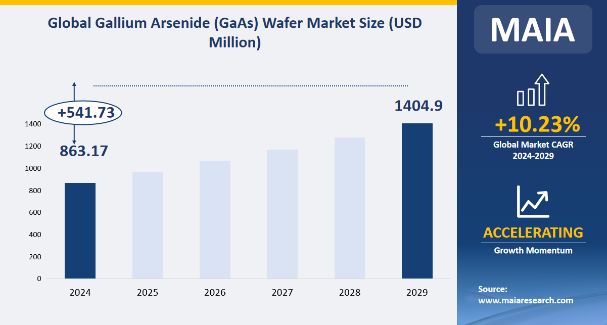
The global gallium arsenide (GaAs) wafer market size will be $863.17 million in 2024 with a CAGR of 10.23% from 2024 to 2029.

Definition
Gallium arsenide (GaAs) is a compound of the element’s gallium and arsenic. It is an III-V direct bandgap semiconductor with a zinc blend crystal structure. Gallium arsenide is used in the manufacture of devices such as microwave frequency integrated circuits, monolithic microwave integrated circuits, infrared light-emitting diodes, laser diodes, solar cells, and optical windows.
Market by Type
Gallium arsenide wafers are manufactured in two different ways, and the LEC technology is used to grow single crystals of materials, especially semiconductors such as gallium arsenide. The crystals are extracted from the melt, which is contained in a suitable crucible and protected from contamination by being encapsulated by the liquid. The VGF process involves carefully controlling the temperature in the furnace to gradually solidify the melt, resulting in the formation of single crystals. The advantage of this method is that the crystals produced are usually of high quality and have a low defect density.
Market by Application
Gallium arsenide (GaAs) wafers are a key component in the manufacture of various electronic devices and can be used in RF, LED, photonics and photovoltaic. Gallium arsenide is a III-V compound semiconductor with a direct band gap that can efficiently emit and absorb light in the infrared and visible spectrum, so it has unique electrical and optical properties that can be used in a variety of devices such as infrared emitting diodes, laser diodes, and microwave frequency integrated circuits. It is also used to produce photovoltaic cells. Gallium arsenide wafers have high electron mobility that surpasses silicon, making them suitable for high-speed applications such as microwave devices, high-speed transistors, and integrated circuits (IC).
Regional Analysis and Insights
Asia Pacific dominates the gallium arsenide (GaAs) wafers market, accounting for a huge revenue share of about 75.4%. It is followed by North America and Europe with shares of 13.5% and 10%, respectively.
Region | Revenue Share in 2024 |
North America | 13.5% |
Europe | 10% |
Asia Pacific | 75.4% |
South America | 0.3% |
Middle East and Africa | 0.8% |
Total | 100% |
Market Opportunities
‘Advantages of gallium arsenide wafer products in semiconductor industry’
Gallium arsenide wafers belong to the semiconductor material industry, is an important part of the upstream semiconductor industry chain, and plays a key role in the production and manufacturing of semiconductor products such as integrated circuits and discrete devices. Gallium arsenide wafer is mainly used as substrate; substrate is the most core material in the field of semiconductor materials. Gallium arsenide has excellent properties as a semiconductor material. Gallium arsenide substrate is used to manufacture semiconductor devices, with high power density, low energy consumption, high temperature resistance, high luminous efficiency, radiation resistance, high breakdown voltage and other characteristics, so gallium arsenide substrate is widely used in the production of LED, RF devices, lasers and other device products. Therefore, the downstream applications of gallium arsenide wafer industry chain mainly involve 5G communication, a new generation of display (Mini LED, Micro LED), unmanned driving, artificial intelligence, wearable devices and other fields. Thanks to the continuous strong demand of downstream applications, the market size of gallium arsenide substrate will continue to expand.
‘The growth of market demand in downstream industries’
Gallium arsenide wafers are one of the mainstream compound semiconductor materials today, originally used in LED and solar cells. With the popularity of mobile devices, gallium arsenide substrates began to be used in the production of RF devices for mobile devices. Gallium arsenide wafers have significant advantages of high electron mobility and high saturated electron rate, so gallium arsenide has been one of the mainstream substrate materials for the manufacture of RF power amplifiers. After entering the 5G era, 5G communication has put forward higher requirements for power, frequency and transmission speed, and RF devices made of gallium arsenide substrate are very suitable for application in high-frequency circuits with long distance and long communication time. Therefore, the material advantages of gallium arsenide are more significant in RF devices in the 5G era. In addition, with the popularity of smart phones and LED, gallium arsenide substrate has entered the stage of large-scale application. For example, in 2017, iPhone X introduced VCSEL for face recognition for the first time. The production of VCSEL requires the use of gallium arsenide substrate, and the application scenario of gallium arsenide substrate has been expanded again. In 2021, with Apple, Samsung, LG, TCL and other manufacturers joining the Mini LED market, the market demand for gallium arsenide substrates will usher in explosive growth.
Top Companies
The gallium arsenide (GaAs) Wafer market is highly competitive and the major players include Sumitomo Electric Industries, Freiberger Compound Materials GmbH, AXT Inc., China Crystal Technologies, DOWA Electronics Materials, Wafer Technology, Atecom Technology Co. Ltd., Powerway Advanced Materials, and Yunnan Germanium.


